I tried to follow this mod instructions: viewtopic.php?t=69578
but it is different than mine, can some one help me on diagram for this tv model?
I attach the chassis details, thank you so much in advance.
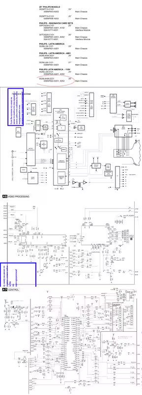

UPDATE: I followed instructions from here: viewtopic.php?t=56155&start=4710
Steps:
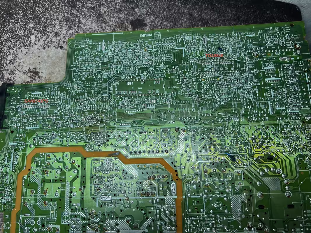
1.- Remove surface mounted resistors at 3675, 3676 and 3677.
2.- At 6603, 6604 and 6605 insert 680R resistor and then a 1N4148 diode on each of these RGB lines. (Resistor closest to micon, then the diode pointed away from micon toward the jungle.)
3.- Leverage the unused J219 header. 5 pin header for R,G,B, blanking and ground (pins 1 through 5, respectively). We will use this to feed in our external RGB and blanking. You need to put the pins in yourself, .1" 5 pin.
4.- The F8 schematic is odd. It shows 100Rs at 3231 (red), 3232 (green) and 3233 (blue) coming out of the header. Elsewhere in the same document it lists zero-ohm resistors in those spots. On my actual PCB, there were no components there at all. They were all gaps that needed to be bridged. So I bridged 5.- the gaps to complete the lines from the header pins to the jungle. I put 270Rs on each of these lines.
6.- For the external RGB lines to feed to the appropriate header pins, do the usual where you have your color lines basically branching, one branch going straight to the correct pin, the other branch connecting to ground through a 75R.
7.- For blanking, I took ~3V from the leg of a capacitor I believe is 2604 (a 22uF cap), to a switch, through a 75R and to pin 4 on J219. You can probably find a better spot to connect than that pin, it works for my design though.
8.- For sync I just fed sync into the composite video input.
Credit to YellowBirdAZ.