A few things first:
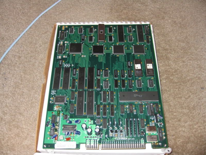
- the large 'EEPROM' which you're referring to (I assume you mean the large chip with the 'window' towards the top of the board) is in fact an EPROM.

- the 'window' on that chip should be covered with a suitable label/sticker - failing to do so means that, over a long period of time, the chip is more likely to be corrupted by UV light (UV light is used to erase EPROMs, but of course in very heavy doses)
The two smaller chips (also EPROMs) which you see with stickers are for the program code - this is the only EPROM/mask ROM code that differs between the International and Japanese version (according to the MAME code) and the large EPROM previously referred to contains some of the graphics.
In theory, it should be possible to program new EPROMs and replace the two that are labelled with the International versions - unless there is some form of protection on the board that prevents this.
So the only question that remains is this - why is an EPROM being used for some of the graphics? Well, the original mask ROM may have failed, or perhaps someone has been modifying some of the graphics (unlikely but possible).
Here's a pic of a board that has a mask ROM in place of the large EPROM on your board:
http://maws.mameworld.info/maws/img/pcb/ddonpach.png
So, in a nutshell, besides putting a label over the 'window' on that large EPROM I would personally leave things as they are.
Note: a mask ROM is read just like an EPROM, but it doesn't have a 'window' on the top and cannot be erased or even programmed by the user. It's manufactured with the internal silicon chip containing the data as specified by the customer. Some of the long, black chips on your board are mask ROMs.
A 'normal' EPROM (or UV-EPROM) requires Ultraviolet light to erase it.
An EEPROM is an electrically eraseable PROM.
http://en.wikipedia.org/wiki/Mask_rom


