It might be that some displays work better with 1080p, particularly if that's their native resolution.
My test displays like x960 for NTSC and x1024 for PAL best.
It'll probably be different again with capture cards, so best try them all


In my memory all systems prior to ps2 had scanlines, but I think I was wrong, now I'm in doubt.AndehX wrote:curious why you would want scanlines on anything higher than 240p? you don't see scanlines on 480i content on a CRT...
There are some ports that are on 480i/480p only systems.AndehX wrote:curious why you would want scanlines on anything higher than 240p? you don't see scanlines on 480i content on a CRT...
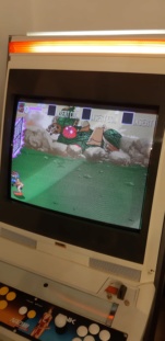
Yes, it's 640x480 on the cabrama wrote:Oh, is that Naomi cabinet 640x480 compatible?
If so, that'd be a reason to keep the 640x480 preset and fix it up a bit.
I've neglected it because I could never find a good use for it.
As a result, it's pretty noisy and the YUV pixels don't align well.
It can be better ;p
Yes, but enabling scanlines on 480i would look very wrong, simply due to the nature of interlaced video.Ryoandr wrote:There are some ports that are on 480i/480p only systems.AndehX wrote:curious why you would want scanlines on anything higher than 240p? you don't see scanlines on 480i content on a CRT...
There are some PC games that can benefit from scanlines
There are some arcade games that are 480i/480p only but use 240p assets.
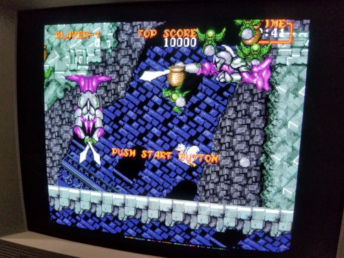
Me too.SuperSpongo wrote:I'd also be interested in an optimized 640x480 setting for my Sony PGM (VGA only)
Right now, I'm using it with the OSSC.

I understand lots has changed. To clarify, has something changed that would affect the ability to access the ESP's wifi? I never had a problem connecting and maintaining a connection, at least as of the May release, and many releases before that.rama wrote:Sure, lots changed, but the problem with the WiFi was always there. It's just that the radio frequency where it blocks the ESP8266 antenna is shifting, depending on the configuration.
Try to connect when your source is off. It should work then.
you can change the wifi channel, or move the antenna physically away from the scalerNoAffinity wrote:I understand lots has changed. To clarify, has something changed that would affect the ability to access the ESP's wifi? I never had a problem connecting and maintaining a connection, at least as of the May release, and many releases before that.rama wrote:Sure, lots changed, but the problem with the WiFi was always there. It's just that the radio frequency where it blocks the ESP8266 antenna is shifting, depending on the configuration.
Try to connect when your source is off. It should work then.
I am able to connect to the wifi with no source, but as soon as I have a source, it goes away. I haven't changed anything with my setup except update to the latest and greatest firmware.
Suggestions?

Code: Select all
  #chip 16F1847

;Define I2C settings

  #define I2C_MODE Master
  #define I2C_DATA PORTA.0
  #define I2C_CLOCK PORTA.1
  #define I2C_ADDRESS 0x2E      ;address of the slave device

;Define Switch and LED ports

  #define LED PORTA.2

;NTSC/PAL Tables

  #include "288p_50Hz_1280x1024.h"

;Set-up

  Dir LED Out
  LED=0

;Set-up variables for use by

  Dim index As Word          ;Parameter Table Index (1-1537)
  Dim seg As Byte             ;Register Segment (Bank 0-5)
  Dim reg As Byte             ;Register Address (0-239)

;====================================================
; MAIN PROGRAM LOOP --- BEGIN
;====================================================

  wait 250 ms
  index = 1                         ;Skip Table Size

  for seg = 0 to 5
    ;----------
    ;       Write to One Control Register TVia5725:
    ;   -Start Signal
    ;   -Slave Address Byte (R/W Bit = Low)
    ;   -Base Address Byte
    ;   -Data Byte to Base Address
    ;   -Stop Signal
    ;----------
    I2CStart
    I2CSend I2C_ADDRESS
    I2CSend 0xF0              ;Point Address to Bank Register
    I2CSend seg               ;Set to New Bank
    I2CStop
    ;----------
    ;     Write to Consecutive Control Registers TVia5725:
    ;  -Start Signal
    ;  -Slave Address Byte (R/W Bit = Low)
    ;  -Base Address Byte
    ;  -Data Byte to Base Address
    ;  -Data Byte to (Base Address + 1)
    ;  -Data Byte to (Base Address + 2)
    ;  -Data Byte to (Base Address + 3)
    ;  -Stop Signal
    ;----------
    I2CStart
    I2CSend I2C_ADDRESS
    I2CSend 0x00                ;Register Base Address
        for reg = 0 to 255
        readtable PAL, index, data
        I2Csend data              ;Data Byte
        index = index+1
        next reg
    I2CStop
  next segment


  Do Forever:
    wait 500 ms
  LED=1
    wait 500 ms
  LED=0
  Loop
Code: Select all
;Default to 8 Mhz internal factory calibrated oscillator

  #chip 16F1847

;Define I2C settings

  #define I2C_MODE Master
  #define I2C_DATA PORTA.0
  #define I2C_CLOCK PORTA.1
  #define I2C_ADDRESS 0x2E      ;address of the TVia5725 Scaler

;Define Switch and LED ports

  #define LED PORTA.2

;NTSC/PAL Tables

  #include "PAL_240P.h"

;Set-up

  Dir LED Out
  LED=0

;Set-up variables for use by

  Dim index As Word          ;Parameter Table Index (1-1537)
  Dim Segment As Byte     ;Register Segment (Bank 0-5)
  Dim Register As Byte      ;Register Address (0-239)

;Sub Routines

Sub I2CBegin
  I2CStart
  I2CSend I2C_ADDRESS
End Sub

Sub WriteByte
  readtable PAL, index, data
  I2Csend data
      index = index+1
End Sub

;====================================================
; MAIN PROGRAM LOOP --- BEGIN
;====================================================

  wait 250 ms
  index = 1                         ;Skip Table Size

  for Segment = 0 to 5
    ;----------
    ;       Write to One Control Register of TVia5725:
    ;   -Start Signal
    ;   -Slave Address Byte (R/W Bit = Low)
    ;   -Base Address Byte
    ;   -Data Byte to Base Address
    ;   -Stop Signal
    ;----------
    Gosub I2CBegin
    I2CSend 0xF0              ;Address Segment (bank) Register
    I2CSend Segment       ;and Set it to Current Segment
    I2CStop
    ;----------
    ;     Write to Consecutive Control Registers of TVia5725:
    ;  -Start Signal
    ;  -Slave Address Byte (R/W Bit = Low)
    ;  -Base Address Byte
    ;  -Data Byte to Base Address
    ;  -Data Byte to (Base Address + 1)
    ;  -Data Byte to (Base Address + 2)
    ;  -Data Byte to (Base Address + 3)
    ;  -Stop Signal
    ;----------
    Select Case Segment

    Case 0                           ;Segment (bank) 0
    Gosub I2CBegin
    I2CSend 0x40               ;Register Base Address
      for Register = 1 to 32
      GoSub WriteByte       ;Send Data
      next Register
    I2CStop
    Gosub I2CBegin
    I2CSend 0x90               ;Register Base Address
      for Register = 1 to 16
      GoSub WriteByte       ;Send Data
      next Register

    Case 1                           ;Segment (bank) 1
    Gosub I2CBegin
    I2CSend 0x00               ;Register Base Address
      for Register = 1 to 48
      GoSub WriteByte       ;Send Data
      next Register

    Case 3                           ;Segment (bank) 3
    Gosub I2CBegin
    I2CSend 0x00               ;Register Base Address
      for Register = 1 to 128
      GoSub WriteByte       ;Send Data
      next Register

    Case 4                           ;Segment (bank) 4
    Gosub I2CBegin
    I2CSend 0x00               ;Register Base Address
      for Register = 1 to 96
      GoSub WriteByte       ;Send Data
      next Register

    Case 5                           ;Segment (bank) 5
    Gosub I2CBegin
    I2CSend 0x00               ;Register Base Address
      for Register = 1 to 112
      GoSub WriteByte       ;Send Data
      next Register

    End Select
    I2CStop
  next Segment


  Do Forever:
    wait 500 ms
  LED=1
    wait 500 ms
  LED=0
  Loop
Code: Select all
;Default to 8 Mhz internal factory calibrated oscillator

  #chip 16F1847

;Define I2C settings

  #define I2C_MODE Master
  #define I2C_DATA PORTA.0
  #define I2C_CLOCK PORTA.1
  #define I2C_ADDRESS 0x2E      ;address of the TVia5725 Scaler

;Define Switch and LED ports

  #define LED PORTA.2

;NTSC/PAL Tables

  #include "PAL_TEST.h"

;Set-up

  Dir LED Out
  LED=0

;Set-up variables for use by

  Dim index As Word          ;Parameter Table Index (1-1537)
  Dim Segment As Byte     ;Register Segment (Bank 0-5)
  Dim Register As Byte      ;Register Address (0-239)

;Sub Routines

Sub I2CBegin
  I2CStart
  I2CSend I2C_ADDRESS
End Sub

Sub WriteByte
  readtable PAL, index, data
  I2Csend data
      index = index+1
End Sub

;====================================================
; MAIN PROGRAM LOOP --- BEGIN
;====================================================

  wait 250 ms
  index = 1                         ;Skip Table Size

  for Segment = 0 to 5
    ;----------
    ;       Write to One Control Register of TVia5725:
    ;   -Start Signal
    ;   -Slave Address Byte (R/W Bit = Low)
    ;   -Base Address Byte
    ;   -Data Byte to Base Address
    ;   -Stop Signal
    ;----------
    Gosub I2CBegin
    I2CSend 0xF0              ;Address Segment (bank) Register
    I2CSend Segment       ;and Set it to Current Segment
    I2CStop
    ;----------
    ;     Write to Consecutive Control Registers of TVia5725:
    ;  -Start Signal
    ;  -Slave Address Byte (R/W Bit = Low)
    ;  -Base Address Byte
    ;  -Data Byte to Base Address
    ;  -Data Byte to (Base Address + 1)
    ;  -Data Byte to (Base Address + 2)
    ;  -Data Byte to (Base Address + 3)
    ;  -Stop Signal
    ;----------
    Select Case Segment

    Case 0                           ;Segment (bank) 0
    Gosub I2CBegin
    I2CSend 0x40               ;Register Base Address
      for Register = 1 to 32
      GoSub WriteByte       ;Send Data
      next Register
    I2CStop
    Gosub I2CBegin
    I2CSend 0x90               ;Register Base Address
      for Register = 1 to 16
      GoSub WriteByte       ;Send Data
      next Register

    Case 1                           ;Segment (bank) 1
    Gosub I2CBegin
    I2CSend 0x00               ;Register Base Address
      for Register = 1 to 48
      GoSub WriteByte       ;Send Data
      next Register

    Case 2                           ;Segment (bank) 1
    Gosub I2CBegin
    I2CSend 0x00               ;Register Base Address
      for Register = 1 to 64
      GoSub WriteByte       ;Send Data
      next Register

    Case 3                           ;Segment (bank) 3
    Gosub I2CBegin
    I2CSend 0x00               ;Register Base Address
      for Register = 1 to 128
      GoSub WriteByte       ;Send Data
      next Register

    Case 4                           ;Segment (bank) 4
    Gosub I2CBegin
    I2CSend 0x00               ;Register Base Address
      for Register = 1 to 96
      GoSub WriteByte       ;Send Data
      next Register

    Case 5                           ;Segment (bank) 5
    Gosub I2CBegin
    I2CSend 0x00               ;Register Base Address
      for Register = 1 to 112
      GoSub WriteByte       ;Send Data
      next Register

    End Select
    I2CStop
  next Segment


  Do Forever:
    wait 500 ms
  LED=1
    wait 500 ms
  LED=0
  Loop


ESP board antenna should be away from any metal plane like ground plane on bottom of GBS.NoAffinity wrote:Esp is stuck to the bottom of the gbs with some 3m velcro adhesive pads, just like it always has been.