CPS2 digital AV interface
-
LordGolem
- Posts: 3
- Joined: Sat Sep 09, 2017 6:35 am
Re: CPS2 digital AV interface
Neat! I'll have to look more into doing this when I get a CPS2 board set one of these days. It looks like something I might be interested in.
Also known as Coreykun667 on Neo-Geo.com forums
-
zeruel85

- Posts: 150
- Joined: Mon Nov 30, 2015 3:47 pm
- Location: Italy
Re: CPS2 digital AV interface
Hi marqs,
I have a question regarding the PCLKx2 signal. I don't understand very well where you take the signal from the motherboard.
Here's a pic of 9S area:
 Thanks in advance for your support.
I have a question regarding the PCLKx2 signal. I don't understand very well where you take the signal from the motherboard.
Here's a pic of 9S area:
Spoiler
-
mikejmoffitt

- Posts: 629
- Joined: Fri Jan 08, 2016 7:26 am
- Location: Tokyo, Japan
-
marqs

- Posts: 1140
- Joined: Sat Dec 15, 2012 12:11 pm
- Location: Finland
Re: CPS2 digital AV interface
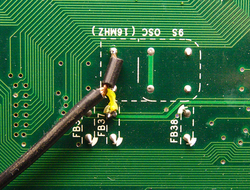
The easiest way is probably to tap the signal directly from oscillator as shown below (pclk_x2 is the yellow wire). I also highly recommend using a coax cable to minimize interference on the clock line.
-
zeruel85
- Posts: 150
- Joined: Mon Nov 30, 2015 3:47 pm
- Location: Italy
Re: CPS2 digital AV interface
Thank you marqs!marqs wrote:The easiest way is probably to tap the signal directly from oscillator as shown below (pclk_x2 is the yellow wire). I also highly recommend using a coax cable to minimize interference on the clock line.
image
BTW watching undamned's video on YT he soldered the coax cable on the top of the motherboard, so I was just curious about that.
-
xterc
- Posts: 19
- Joined: Sat Aug 05, 2017 12:38 am
Re: CPS2 digital AV interface
This board looks great. I am going to get one made for myself once the next revision is posted. However, if I'm going to get one made I might as well get 10 built. I know this is open source, but if someone sells these for profit (or integrates one into a consolized CPS2 for re-sale), is there an arrangement where a % is returned to Marqs?
The S25FL116K flash memory referenced in the BOM (S25FL116K0XMFI041) is obsolete, on a cursory glance it looks like S25FL116K0XMFA041 is compatible and can be substituted, can someone confirm?
The S25FL116K flash memory referenced in the BOM (S25FL116K0XMFI041) is obsolete, on a cursory glance it looks like S25FL116K0XMFA041 is compatible and can be substituted, can someone confirm?
-
marqs
- Posts: 1140
- Joined: Sat Dec 15, 2012 12:11 pm
- Location: Finland
Re: CPS2 digital AV interface
IS25LP016D-JNLE-TR can be used as a replacement for S25FL116K.xterc wrote:The S25FL116K flash memory referenced in the BOM (S25FL116K0XMFI041) is obsolete, on a cursory glance it looks like S25FL116K0XMFA041 is compatible and can be substituted, can someone confirm?
-
xterc
- Posts: 19
- Joined: Sat Aug 05, 2017 12:38 am
Re: CPS2 digital AV interface
Thanks for the reply, I appreciate it. Is there any word if there will be a new rev of the board any time soon, or has this project been put on the back-burner?
-
zeruel85
- Posts: 150
- Joined: Mon Nov 30, 2015 3:47 pm
- Location: Italy
Re: CPS2 digital AV interface
If someone is interested, I ordered a little batch of v1.0 PCBs.
I will have 3x PCBs available in about 3/4 weeks (including components not assembled).
I will have 3x PCBs available in about 3/4 weeks (including components not assembled).
-
xterc
- Posts: 19
- Joined: Sat Aug 05, 2017 12:38 am
Re: CPS2 digital AV interface
Definitely, I've not pulled the trigger yet on getting the board made locally. Let me know how much!zeruel85 wrote:If someone is interested, I ordered a little batch of v1.0 PCBs.
I will have 3x PCBs available in about 3/4 weeks (including components not assembled).
-
mtn360
- Posts: 63
- Joined: Sat Apr 15, 2017 1:51 am
- Location: Australia
- Contact:
Re: CPS2 digital AV interface
I'd surely love to get my hands on one of these for my Darksoft kit. If somebody of you would have an A board spare, I'd love to pay for that as well, plus installation (whatever you consider fair) + posting costs to Australia. My soldering skills got real rusty and never been great :-/ Happy to pay upfront/right away of course. Otherwise I'd also try things myself with a spare A board of mine.
xterc wrote:Definitely, I've not pulled the trigger yet on getting the board made locally. Let me know how much!zeruel85 wrote:If someone is interested, I ordered a little batch of v1.0 PCBs.
I will have 3x PCBs available in about 3/4 weeks (including components not assembled).
Current projects
https://fullset.io - New games for Neo Geo (Project Neon, Overserved: Food Fighters!)
https://sumthings.com - Buy, Track & Sell your favorite Retro & Arcade Games.
https://fullset.io - New games for Neo Geo (Project Neon, Overserved: Food Fighters!)
https://sumthings.com - Buy, Track & Sell your favorite Retro & Arcade Games.
-
marqs
- Posts: 1140
- Joined: Sat Dec 15, 2012 12:11 pm
- Location: Finland
Re: CPS2 digital AV interface
I originally intended to design the new rev PCB last month, but I've started to look if the board could be easily made to support CPS3 (and possibly original CPS) as well.xterc wrote: Is there any word if there will be a new rev of the board any time soon, or has this project been put on the back-burner?
-
modology

- Posts: 32
- Joined: Tue May 17, 2016 3:17 pm
Re: CPS2 digital AV interface
@RGB
I do hope that once the design becomes available for public, i do hope to see HAS Supergun has AV Digital as well.
I do hope that once the design becomes available for public, i do hope to see HAS Supergun has AV Digital as well.
-
marqs
- Posts: 1140
- Joined: Sat Dec 15, 2012 12:11 pm
- Location: Finland
Re: CPS2 digital AV interface
Some CPS3 details from a couple measurements:
PCLK: ~8.59MHz (42.9545MHz/5)
Scanlines: 264
Dots per scanline: 546
Active width: 384 (more in 16:9 mode)
Refresh rate: ~59.60Hz
Audio sample rate: 37.3kHz (42.9545MHz/(3*384))
Video could be processed even by current cps2_digiav board, but 37.3kHz audio is a bummer. It's far from a simple task to implement asynchronous sample-rate conversion on FPGA, so only viable option I can think of is adding a dedicated ASRC chip (e.g. from SRC419x or AD189x series) on the upcoming PCB. The PCB can be still designed so that ASRC chip can be left out if installed on CPS2.
-
undamned

- Posts: 3273
- Joined: Sat Jan 29, 2005 9:27 am
- Location: Phoenix
Re: CPS2 digital AV interface
I think that's a reasonable strategy. I'm guessing CPS3 demand will be fairly small compared to CPS2 (but having cross-platform capability will be excellent).marqs wrote:Some CPS3 details from a couple measurements:
...
37.3kHz audio is a bummer. It's far from a simple task to implement asynchronous sample-rate conversion on FPGA, so only viable option I can think of is adding a dedicated ASRC chip (e.g. from SRC419x or AD189x series) on the upcoming PCB. The PCB can be still designed so that ASRC chip can be left out if installed on CPS2.
-ud
Righteous Super Hero / Righteous Love
-
DewmanSNK
- Posts: 16
- Joined: Wed Nov 12, 2008 6:32 am
Re: CPS2 digital AV interface
https://github.com/wifiber/cps2_digiav/tree/develmarqs wrote:...The PCB still needs 1-2 revisions before it can be considered release quality. Ideally it could be fitted inside CPS2 case with just one extra hole for HDMI connector. Board design files, gerbers, firmware etc. will all be freely available once the project is more mature. Below is a couple photos of the current prototype (click for bigger versions).
I have forked the repository and made a few changes. I wanted the board to be a daughter-board that fit on top of the 24-pin DIPs in the CPS2 mainboard, and output the HDMI via a small cutout near the volume buttons. I also have moved all the larger ICs to the top of the board. This will allow the board to be assembled in my re-flow oven. With my OSSC experience, I found the surface tension of the solder could hold the SOT-23-5 voltage regulators and the small passive components, but nothing much bigger than that. I just finished layout and routing last night, so the silk screen (values, references) needs to be corrected. ALSO, I was forced to move the pin assignments for the 4-bit color (R,G,B,F) - this will require a change to the pin assignments in the FPGA (I know its a UCF file in Xilinx land, cant remember what Altera/Intel call it) I did leave the external clock and V/H sync pin assignments as they were, since those go to global clock lines on the FPGA.
I am planning on update the silk screen layer and modifying the code in the FPGA to take account of the new pin assignments. I wish I would have been paying closer attention to this thread as Marqs laid out some plans for part changes and improving the design, that I wish I would have rolled into my new layout. At any rate, I was going to finish this board up this week and decide if I should go ahead and make the board, or try and incorporate some of the part and design changes that Marqs recommended and hold off on making a board till all those component changes are complete.
Having the HDMI connector near the volume buttons wasn't my first choice, but it seemed like a decent compromise to have the PCB be a daughter board on the 24-pin DIPs, and I can also leverage a plastic post inside the CPS2 to provide some structural support for the PCB when HDMI cables are connected and removed.
https://imgur.com/a/il4zv
The 3D model is a bit misleading - the J1 J2 DIP packages are shown as ICs, these will be pin-headers in reality that mate with DIP sockets that will be piggy-backed on the 24 pin DIPs in the CPS2. Also the HDMI connector is missing, but easy to guess where it goes. I have measured my CPS2 A-board several times and THINK - I have the spacing correct for the J1/J2 DIPs and the strain relief hole in the bottom corner, and the HDMI connector - but if someone wants to double check my work - that would be super helpful.
-
zeruel85
- Posts: 150
- Joined: Mon Nov 30, 2015 3:47 pm
- Location: Italy
Re: CPS2 digital AV interface
I have 2x (maybe 3x) CPS2_digiAV v1.0 available right now.
You can buy a DIY kit or a pre-assembled one, I have all the components, not only the PCBs.
Contact me via PM if you are interested in them, thank you.


You can buy a DIY kit or a pre-assembled one, I have all the components, not only the PCBs.
Contact me via PM if you are interested in them, thank you.
-
nio
- Posts: 39
- Joined: Thu Apr 16, 2015 12:18 pm
Re: CPS2 digital AV interface
will it also work with neo geo?
-
Shin

- Posts: 95
- Joined: Thu Mar 01, 2007 5:17 pm
- Location: Strasbourg, France(?)
Re: CPS2 digital AV interface
Impressive stuff.(was especially impreessed by the lag video) Would definitely be down for one for me CPS3. (don't own other arcade system yet)
I know it would drive the price up, but I guess it would be interesting to make the board with a socket, especially if the board can be adapted on all 3 CPS. (would a single fw work on all 3 or would the fw need to be reprogrammed to work for each system ?) also if one wants to upgrade later with a new board with a new fpga (4K compatibilty ?)
I guess no FPGA dev board supports 4K and HDMI 2.1 right now, but would Variable Refresh Rate and Quick Frame Transport for the HDMI 2.1 standard help with unconventinal arcade bound refresh rates and funky refresh issues like with the nes/snes ?
thanks a lot for you work btw !
-
marqs
- Posts: 1140
- Joined: Sat Dec 15, 2012 12:11 pm
- Location: Finland
Re: CPS2 digital AV interface
Video path should be fine for Neo Geo if digital RGB bus is available on its mainboard. Cps2_digiav is designed to support I2S sound input, so if Neo Geo uses another digital audio interface then it's harder to support.nio wrote:will it also work with neo geo?
There's not too many solder points and the board is easy to install overall, so there would not be huge benefits using a socket (which should also somehow be tightly installable on the arcade board). Firmware needs to be separate for each supported system.Shin wrote:I know it would drive the price up, but I guess it would be interesting to make the board with a socket, especially if the board can be adapted on all 3 CPS. (would a single fw work on all 3 or would the fw need to be reprogrammed to work for each system ?) also if one wants to upgrade later with a new board with a new fpga (4K compatibilty ?)
The only potential help I see from VFR is that compliant displays should accept refresh rates like 59.63Hz without any issue (possibly in non-VFR mode too, in which case the source would not even need to be HDMI 2.1 -capable).Shin wrote:I guess no FPGA dev board supports 4K and HDMI 2.1 right now, but would Variable Refresh Rate and Quick Frame Transport for the HDMI 2.1 standard help with unconventinal arcade bound refresh rates and funky refresh issues like with the nes/snes ?
-
xterc
- Posts: 19
- Joined: Sat Aug 05, 2017 12:38 am
Re: CPS2 digital AV interface
I also got some of Marq's boards made. I'm still waiting on components to come in. In the mean-time I've been practicing SMD soldering with a practice board (also pictured).

-
Aleyr

- Posts: 7
- Joined: Sun Jan 07, 2018 4:41 am
Re: CPS2 digital AV interface
Marqs can the same replacement can be done for the OSSC board too?marqs wrote:IS25LP016D-JNLE-TR can be used as a replacement for S25FL116K.xterc wrote:The S25FL116K flash memory referenced in the BOM (S25FL116K0XMFI041) is obsolete, on a cursory glance it looks like S25FL116K0XMFA041 is compatible and can be substituted, can someone confirm?
-
marqs
- Posts: 1140
- Joined: Sat Dec 15, 2012 12:11 pm
- Location: Finland
Re: CPS2 digital AV interface
Yes, you can use it for OSSC too.Aleyr wrote:Marqs can the same replacement can be done for the OSSC board too?marqs wrote:IS25LP016D-JNLE-TR can be used as a replacement for S25FL116K.xterc wrote:The S25FL116K flash memory referenced in the BOM (S25FL116K0XMFI041) is obsolete, on a cursory glance it looks like S25FL116K0XMFA041 is compatible and can be substituted, can someone confirm?
-
modology
- Posts: 32
- Joined: Tue May 17, 2016 3:17 pm
Re: CPS2 digital AV interface
any update on adapting it over for cps3?
-
marqs
- Posts: 1140
- Joined: Sat Dec 15, 2012 12:11 pm
- Location: Finland
Re: CPS2 digital AV interface
I'm just about to start integrating DewmanSNK's changes with my own to move the updated PCB design forward. It will have a slightly bigger FPGA (CPS3 widescreen mode requires extra line buffer space), Si5351C clock generator (CEA-1080p), ADV7513 HDMI transmitter (better availability), SRC4190 sample rate converter IC (for CPS3 audio) and a few other small changes.modology wrote:any update on adapting it over for cps3?
-
zeruel85
- Posts: 150
- Joined: Mon Nov 30, 2015 3:47 pm
- Location: Italy
Re: CPS2 digital AV interface
Hey marqs,marqs wrote:I'm just about to start integrating DewmanSNK's changes with my own to move the updated PCB design forward. It will have a slightly bigger FPGA (CPS3 widescreen mode requires extra line buffer space), Si5351C clock generator (CEA-1080p), ADV7513 HDMI transmitter (better availability), SRC4190 sample rate converter IC (for CPS3 audio) and a few other small changes.modology wrote:any update on adapting it over for cps3?
should CEA-1080p solve compatibily issues with my Asus VX279H display?
Do you remember my 'Out of Range' behaviour?
By the way, I tried to manage with DVDO settings, but I cannot figure it out always Unknown input signal and a solid blue screen (typical when DVDO does not hang the signal).
Thanks for your update.
-
marqs
- Posts: 1140
- Joined: Sat Dec 15, 2012 12:11 pm
- Location: Finland
Re: CPS2 digital AV interface
The new design should be compatible as long as connected display supports CPS2/CPS3 refresh rate.zeruel85 wrote:should CEA-1080p solve compatibily issues with my Asus VX279H display?
Do you remember my 'Out of Range' behaviour?
That's strange considering DVDOs support OSSC line5x which should be very close.zeruel85 wrote:By the way, I tried to manage with DVDO settings, but I cannot figure it out always Unknown input signal and a solid blue screen (typical when DVDO does not hang the signal).
-
xterc
- Posts: 19
- Joined: Sat Aug 05, 2017 12:38 am
Re: CPS2 digital AV interface

It's probably not a big deal for most people on here, but I've started to put the CPS2_digAV together and I'm really enjoying SMD soldering. Hopefully everything will be completed by the end of the month.
-
DewmanSNK
- Posts: 16
- Joined: Wed Nov 12, 2008 6:32 am
Re: CPS2 digital AV interface
Looking good! Be careful when you solder the FPGA, the pins are really fragile and I had legs bend over when doing the drag soldering, cost me an OSSC in the past.xterc wrote:
It's probably not a big deal for most people on here, but I've started to put the CPS2_digAV together and I'm really enjoying SMD soldering. Hopefully everything will be completed by the end of the month.
-
mikejmoffitt
- Posts: 629
- Joined: Fri Jan 08, 2016 7:26 am
- Location: Tokyo, Japan
Re: CPS2 digital AV interface
If you want to try Neo-Geo support I have mapped out the RGB breakout for multiple boards.
The main issue is for HDMI audio you have digital audio as well as analogue audio coming from the YM2610. It would maybe be easier to just reimplement the SSG portion of that chip in HDL and tap the bus, to avoid having to do ADC.
http://mikejmoffitt.com/neovga/diagrams/
The main issue is for HDMI audio you have digital audio as well as analogue audio coming from the YM2610. It would maybe be easier to just reimplement the SSG portion of that chip in HDL and tap the bus, to avoid having to do ADC.
http://mikejmoffitt.com/neovga/diagrams/